


-

- Columns
- Failure analysis method for semiconductor devices and precision modules
Capabilities
Failure analysis method for semiconductor devices and precision modules
Share


Thorough failure analysis enables high yields, even in contract manufacturing.
1. The Importance of PCBA Failure Analysis
Non-destructive analysis is an important failure analysis method for semiconductor devices, precision modules, and other devices.
Even if a product is disassembled after a failure occurs, it is difficult to reproduce the symptoms or identify the exact location of the failure.
Therefore, we first narrow down the failure location and identify the cause in the product’s original state, and then proceed with physical analysis to determine the true cause.
2. Example of Failure Analysis Procedure
Non-destructive testing begins with an external appearance check.
The presence or absence of stress marks, such as dents or scratches on the product’s periphery, provides important clues.
Next, electrical characteristic analysis is performed to identify open cracks in the semiconductor device, open electrical junctions, shorts, and the exact location of the failure.
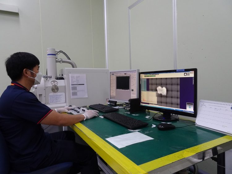
Once the problem has been narrowed down to a certain extent through electrical analysis, the internal structure is examined using techniques such as X-rays and SEM observation.
Once the symptoms and location of the failure have been identified, the product is carefully disassembled and physical analysis is performed to determine the cause of the failure.
3. Passing on Failure Analysis Skills
As mentioned above, in addition to the appropriate equipment, failure analysis relies on the insight, reasoning, and intuition of the analyst.
By passing on the skills we have cultivated over our many years of experience, including those of our analysts who investigate the causes of defects and develop countermeasures, we have established a system that enables us to maintain high yields and high quality.
Share
Popular Columns
-
 17/08/2026
WSE's work environment, benefits, and personal impressions
Workplace
-
15/06/2026
Contract Manufacturing Hub in Southern Vietnam: The Charm of Ho Chi Minh City and the Strengths of WSE - Part 1
Vietnam Trends
-
 19/01/2026
Advantages/Superiority of WSE Production from the Japanese Perspective – Part 2
Vietnam Trends
-
 19/10/2026
Failure analysis method for semiconductor devices and precision modules
Capabilities
-
20/07/2026
Contract Manufacturing Hub in Southern Vietnam: The Charm of Ho Chi Minh City and the Strengths of WSE - Part 2
Vietnam Trends
Related Columns
-
21/09/2026
設備は生産性を生み、人は信頼を生む
Capabilities
-
18/05/2026
OEM system that meets customer needs through domestic and international collaboration
Capabilities
-
20/04/2026
SUN-S/WSE Production Technology Capabilities and Advantages - Part 2
Capabilities
-
16/03/2026
SUN-S/WSE Production Technology Capabilities and Advantages - Part 1
Capabilities
-
 16/02/2026
Manufacturing of camera modules for mobile phones
Capabilities